Tour 1: Leibniz-Institut für Kristallzüchtung (IKZ)
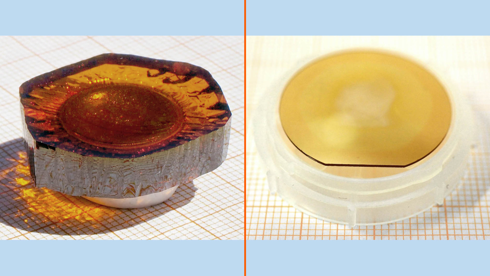
Aluminium Nitride Substrates for UVC Light Emitting Diodes and other crystalline materials
The Leibniz-Institut für Kristallzüchtung (IKZ) in Berlin-Adlershof is an international state-of-the-art competence center for science & technology as well as service & transfer for innovations in and by crystalline materials. The R&D spectrum thereby ranges from basic over applied research activities up to pre-industrial research tasks.
Crystalline materials are key technology enabling components to provide electronic and photonic solutions to today´s and future challenges in society such as artificial intelligence (communication, mobility etc.), energy (renewable energies, power conversion etc.) and health (medical diagnosis, modern surgical instruments etc.).
The tour includes a short presentation of activities on aluminium nitride bulk crystal growth and substrate preparation at IKZ including a visit of the growth equipment and preparation laboratories. Additionally, activities on other semiconductor material like silicon or various oxides grown from the melt will be shown.

- Min. number of participants: 5
- Max. number of participants: 10
- Meeting Point & Time: Hotel Lobby, 09:00
Due to COVID-19 and other communicable diseases, access may be restricted. There are currently no access restrictions for this location, but requirements are subject to change.
Leibniz-Institut für Kristallzüchtung (IKZ)
Max-Born-Straße 2
12489 Berlin, Germany
► Further information on Leibniz-Institut für Kristallzüchtung (IKZ)